


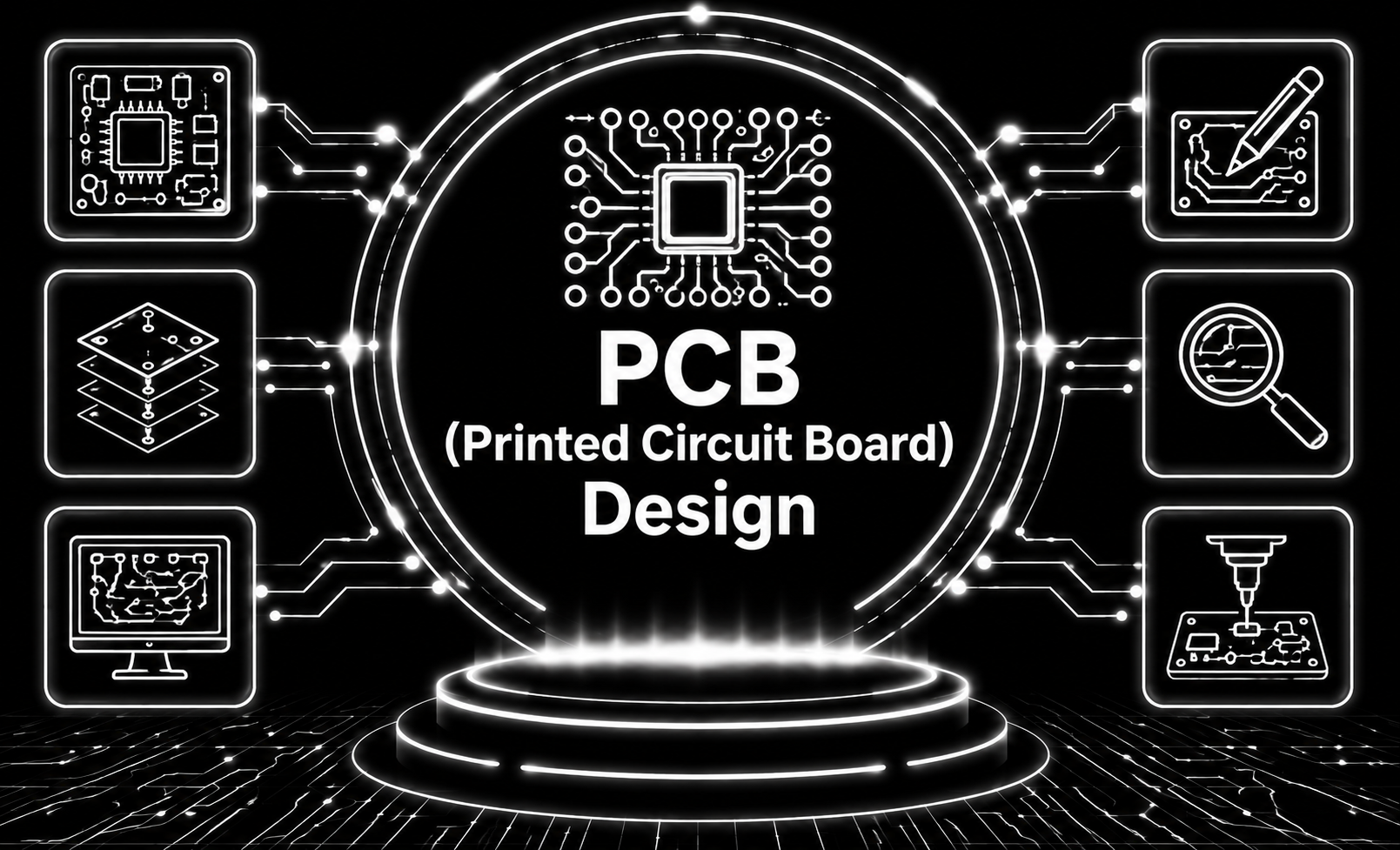
PCB (Printed Circuit Board) Design focuses on developing the detailed circuit layouts that form the backbone of electronic devices. This includes schematic creation, component selection, board routing, layer planning, and signal integrity optimization. Designers ensure proper placement of components, controlled impedance, thermal management, and EMI/EMC compliance to guarantee stable and safe operation. The service also prepares manufacturing files (Gerber, BOM, drill files) and supports prototype testing, revisions, and production optimization. Whether for IoT devices, consumer electronics, industrial equipment, or custom hardware, high-quality PCB design ensures the device is reliable, efficient, and ready for scalable manufacturing.
PCB (Printed Circuit Board) Design
Built on Trusted Technologies
At Capnis, we work with modern, industry-trusted technologies that power fast development, strong security, and reliable performance across all projects.

Altium Designer
A professional PCB design suite offering schematic capture, layout, simulation, and manufacturing-ready output.

KiCad
An open-source PCB design tool with schematic editing, 3D visualization, and multi-layer board support.

Eagle (Autodesk Eagle)
A widely used PCB design tool featuring schematic capture, autorouting, and a large component library.

OrCAD
High-end enterprise PCB design and simulation tools suitable for complex, high-speed, and multi-layer boards.

EasyEDA
A web-based PCB design tool supporting schematics, layouts, libraries, and direct JLCPCB fabrication integration.

Fritzing
A beginner-friendly PCB and electronics prototyping tool for hobbyists and makers.

Proteus Design Suite
A design environment combining schematic capture, PCB layout, and microcontroller simulation.

CircuitMaker
A community-driven PCB design tool from Altium offering professional-grade features for free.

Mentor Graphics PADS
A professional PCB design system with powerful layout and high-speed routing capabilities.
Services
Growing sales through exceptional services

Discover What We Deliver
Printed Circuit Board Design
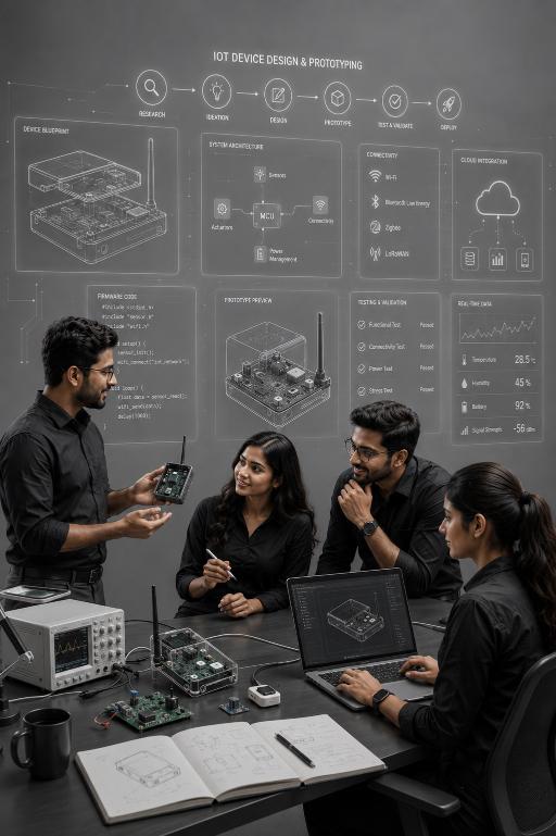
PCB (Printed Circuit Board) Design is a critical component of IoT development, serving as the foundation for connecting and integrating electronic components in IoT devices.Built for Your Business
Our services are designed to address real-world business challenges through a practical, results-driven approach. We focus on understanding your requirements, delivering reliable execution, and ensuring ongoing support to help your business operate efficiently and grow with confidence.
Capnis InfoTech Private Limited

Service Questions
PCB Design is important in IoT development as it determines the performance, size, and reliability of IoT devices. A well-designed PCB layout can optimize signal integrity, reduce size, and enhance reliability, leading to better overall device performance.
Factors to consider in PCB Design for IoT devices include signal integrity, power distribution, thermal management, component placement, size constraints, and manufacturability.
Custom PCB Design enables IoT developers to create tailored hardware solutions optimized for their specific applications, resulting in improved performance, reduced size, lower manufacturing costs, and faster time to market.

BlueRiver Analytics – CEO: Priya Deshmukh
Client
★
★
★
★
★
““Capnis delivered an exceptional PCB design that met all our technical and performance requirements. Their team demonstrated impressive precision, creating a layout that was efficient, reliable, and production-ready. They optimized component placement and routing to ensure high-quality electrical performance. Communication was smooth throughout, with every revision handled promptly and professionally. We highly recommend Capnis for expert and dependable PCB design services.””
Request a quote
Three quick steps—your details, scope & timing, then budget. We route PCB (Printed Circuit Board) Design requests to the right delivery lead with full context.